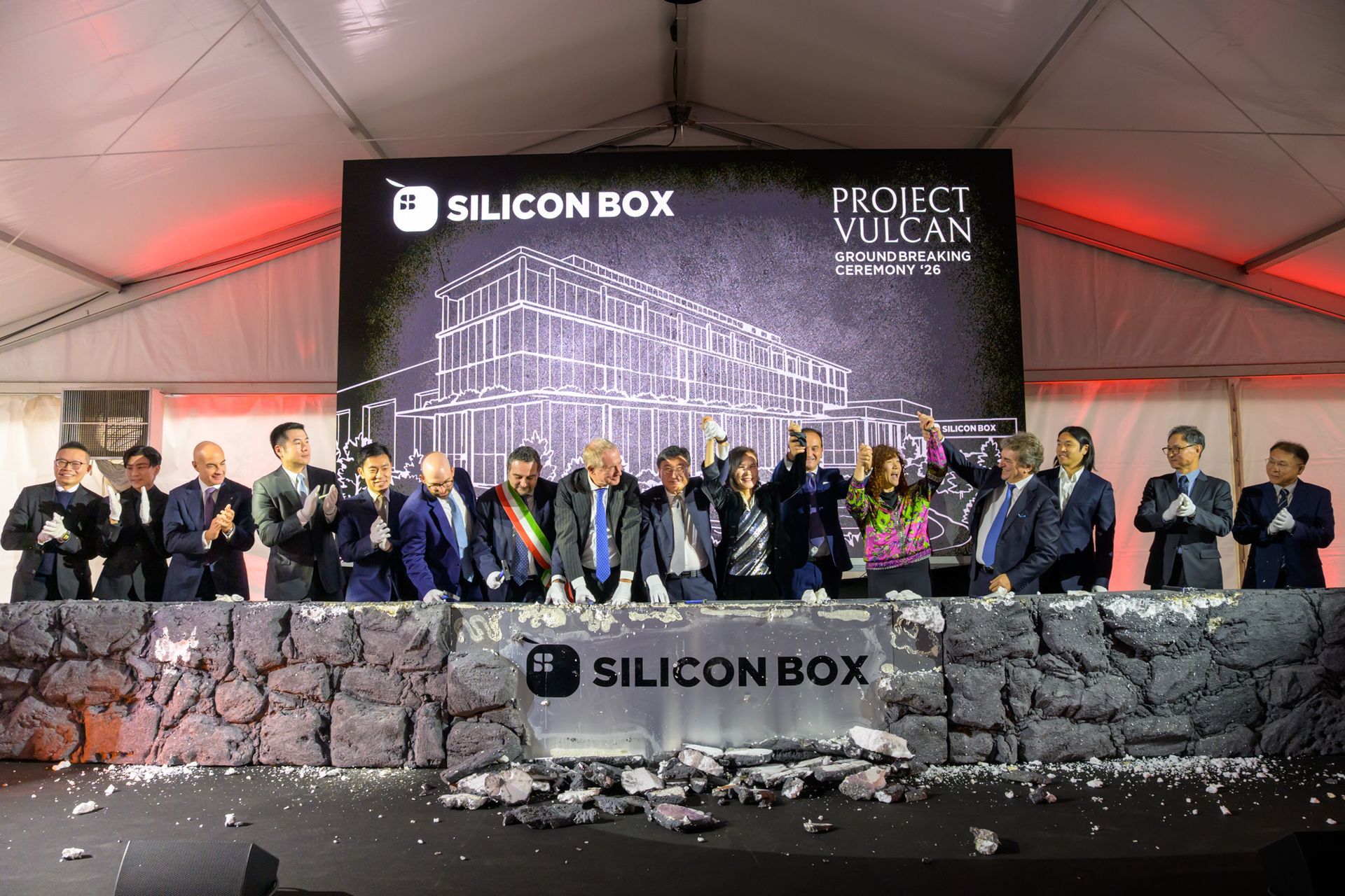
Silicon Box semiconductor manufacturing facility in Italy enters Basic Design phase
Supported by Stantec and Drees & Sommer, the project will be the first of this kind in Europe and will help strengthen Europe’s semiconductor supply chain.
NOVARA, ITALY, November 16, 2026 -- Silicon Box, a leader in chiplet integration and advanced packaging for semiconductors, has moved its €3.2 billion assembly and test facility in Novara, Northern Italy, into the Basic Design phase. The milestone was reached together with its design and engineering partners Stantec, a global leader in sustainable design and engineering, and Drees & Sommer, an international consulting and engineering firm.
Once complete, the facility will provide advanced semiconductor assembly and testing to support long-term growth, foster innovation, and strengthen chip supply chain resilience in Italy and Europe. It marks Silicon Box’s first manufacturing expansion outside Singapore and the first plant of this type in Europe. Using highly innovative technology already deployed in Singapore, it will integrate and test chiplets of different sizes from multiple manufacturers on a single platform, delivering greater flexibility, scalability, and performance.
The firms were appointed by Silicon Box in 2025 to provide multidisciplinary design and engineering services for the new facility. Stantec leads overall project coordination, architectural and landscape design for the office building and external areas, infrastructure design, water and power supply, and permitting and authorization services. Drees & Sommer is responsible for the integrated design of the production and utility buildings, combining CSA (Civil, Structure and Architecture) and MEP (Mechanical, Electrical, Plumbing) disciplines with specialist cleanroom design to align the facility’s buildings with Silicon Box’s advanced manufacturing requirements.
For Silicon Box, the Basic Design phase is where the experience of its Singapore operations is built into the Novara plant. "Our Singapore facility has shown that advanced panel-level packaging can run at high volume and at high yield. Our task now is to build that same discipline into Novara from the first drawing," said Jae Hak "JH" Yee, Chief Operating Officer at Silicon Box. "Working closely with Stantec and Drees & Sommer, we are making sure that production flows, cleanrooms and utility systems are designed around how the plant will actually operate. The fast-track schedule lets us move quickly toward construction in 2027, while our focus stays on a facility that our customers and our future Italian workforce can rely on for the long term."
“The transition to Basic Design marks an important step in turning Silicon Box’s vision into a deliverable industrial project,” said Emanuela Sturniolo, operations director for Stantec in Italy. “This investment will create long-term technological, economic, and skills value for Italy while contributing to Europe’s semiconductor ambitions. Stantec can leverage its international expertise with local knowledge to help move this highly complex project forward.”
“In a project of this scale and technical complexity, the value of specialist engineering lies in a facility that supports demanding production processes while remaining efficient and adaptable over time,” said Silvia Turtschan, head of CoC semiconductor and Associate Partner at Drees & Sommer. “In a globally competitive semiconductor industry, this adaptability is essential to keeping pace with technological change and supporting long-term competitiveness.”
Advancing industrial development in Italy's Piedmont region
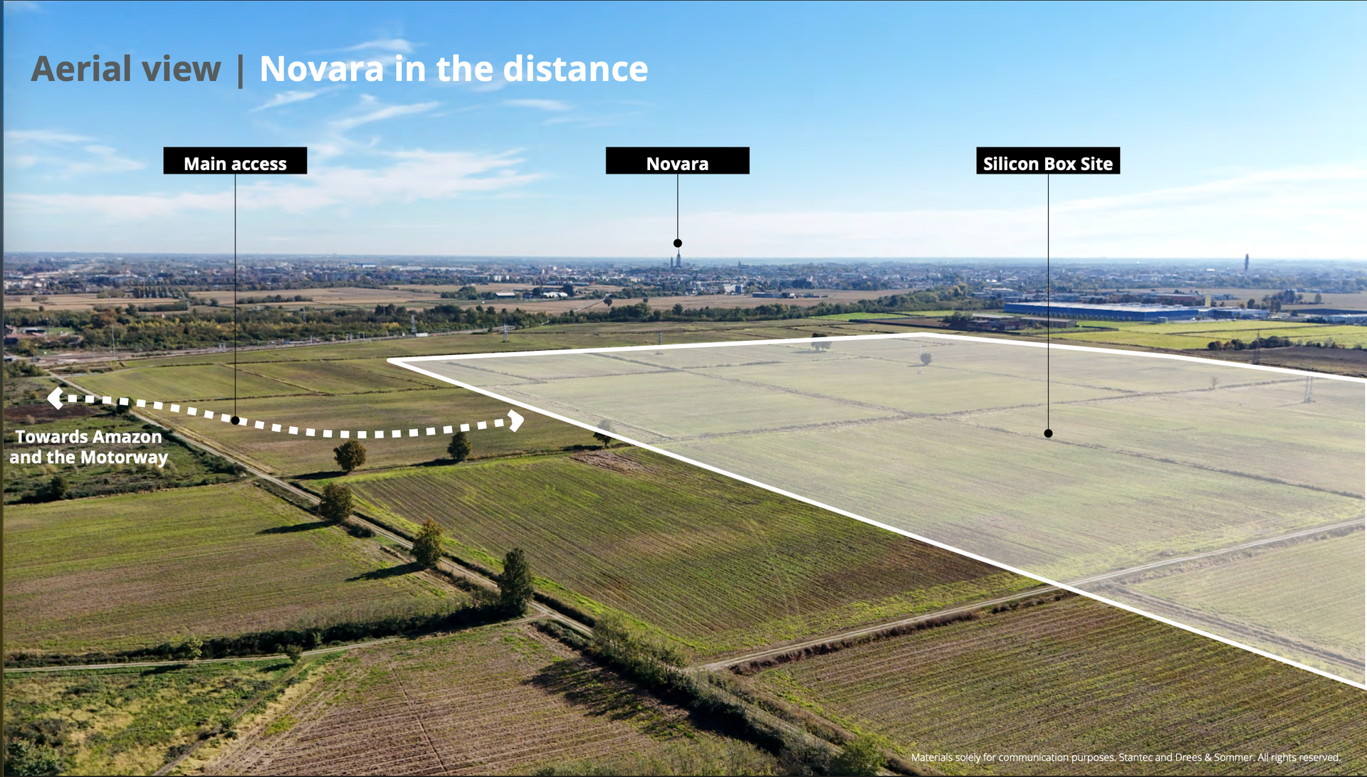
From the earliest stages of the project, environmental and landscape considerations have shaped the design that respects and reflects the distinctive character of the local Piedmont plain. The facility will occupy a 60-hectare site in the province of Novara, an area experiencing significant industrial and infrastructure development. Direct access to the recently completed Agognate railway station connects the campus to Novara city centre in just a few minutes, supporting the broader strategy of promoting sustainable mobility solutions.
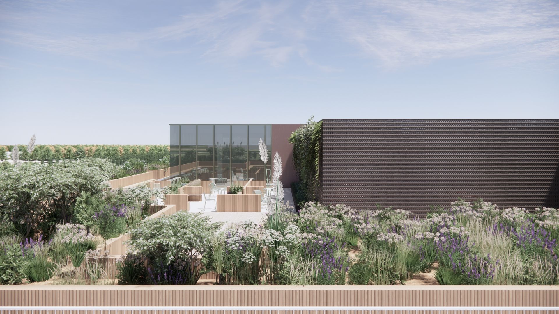
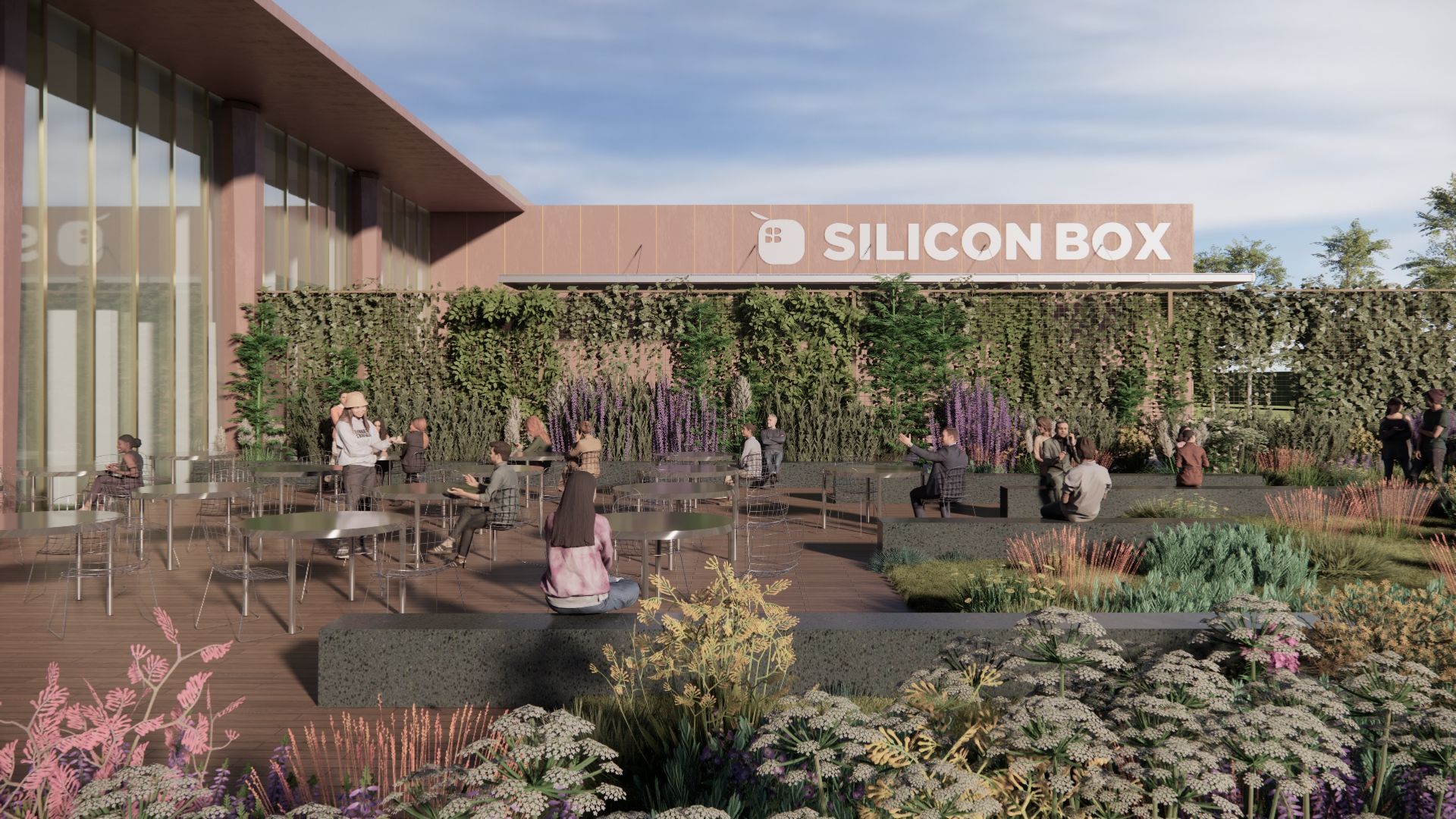
The architectural concept proposed by the Stantec team for the main building connects landscape and technology, housing representative spaces, research and development facilities, and administrative functions. Its exterior draws inspiration from the Novara countryside, while the interiors combine technical precision with the warmth and craftsmanship of Italian design. The masterplan is conceived as a flexible and adaptable framework for future growth, capable of evolving over time in response to continuous developments in the market, technology, and production systems.
Drees & Sommer’s design approach for production areas and buildings housing auxiliary systems is based on advanced semiconductor manufacturing processes and their specific technical requirements. Cleanroom environment, equipment interfaces, material and personnel flows, structural solutions, and mechanical and electrical systems are developed as an integrated whole. This integration will provide a robust technical basis for subsequent project stages, supporting reliable operations and future adaptability through Basic Design.
Designed for place and performance
The landscape strategy aims to integrate the site harmoniously into the Novara landscape, transforming mitigation measures into a multifunctional green infrastructure that enhances biodiversity, manages stormwater sustainably, and maximizes soil permeability without affecting surrounding areas. Open spaces will support employee well-being and welcome the local community, extending the project’s environmental and social benefits to the wider area.
Stantec’s sustainability approach sets high environmental standards to reduce the facility’s environmental footprint. Proposed measures include water reuse, process heat recovery through high-efficiency systems, photovoltaic energy, and nature-based solutions integrated into the overall landscape strategy to enhance climate resilience.
Drees & Sommer’s design strategy focuses on performance throughout the facility’s operational life. Production and utility areas are designed to deliver stable, high-performance operating conditions, optimize energy and water use, and sustain the facility’s competitiveness as semiconductor technologies evolve. This lifecycle-oriented approach aims to provide Silicon Box with a resilient industrial asset that combines high technical performance with long-term operational value.
Silicon Box’s new semiconductor assembly and test facility is set to boost Italy’s high-tech manufacturing ecosystem, attract further investment, and strengthen national capabilities in fast-growing sectors for future technologies.
DISCLAIMER: These materials are provided solely for communication purposes and do not constitute contractual design documentation; the final design may change as the project progresses and is subject to regulatory and other requirements. Use is restricted to press communications, and no party should rely on these materials for any other purpose; no liability is accepted for such reliance.
About Silicon Box
Silicon Box is an advanced semiconductor packaging company, specializing in cutting-edge integration technology and manufacturing processes. We offer solutions that enable chiplet architecture, as well as high-performance, affordable alternatives to traditional packaging schemes. Leveraging our proprietary technology, 30 years of multi-sectoral expertise, and relationships with best-in-class partners, we strive to solve the unique challenges of chiplet adoption to build the emergent technologies shaping the world around us today. Silicon Box was founded in 2021 by Dr. Byung Joon (BJ) Han, Dr. Sehat Sutardja, and Weili Dai. To learn more about Silicon Box, visit silicon-box.com/newsroom and silicon-box.com/timeline.
About Stantec
Stantec empowers clients, people, and communities to rise to the world’s greatest challenges at a time when the world faces more unprecedented concerns than ever before. We are a global leader in sustainable engineering, architecture, and environmental consulting. Our professionals deliver the expertise, technology, and innovation communities need to manage aging infrastructure, demographic and population changes, the energy transition, and more. Today’s communities transcend geographic borders. At Stantec, community means everyone with an interest in the work that we do—from our project teams and industry colleagues to our clients and the people our work impacts. The diverse perspectives of our partners and interested parties drive us to think beyond what’s previously been done on critical issues like climate change, digital transformation, and future-proofing our cities and infrastructure. We are designers, engineers, scientists, project managers, and strategic advisors. We innovate at the intersection of community, creativity, and client relationships to advance communities everywhere, so that together we can redefine what’s possible. Stantec trades on the TSX and the NYSE under the symbol STN. Visit us at stantec.com or find us on social media. Learn more about Stantec’s innovative industrial building design solutions.
About Drees & Sommer
Drees & Sommer is a partner-managed, global consulting company that provides a single source of consultation and implementation services. We focus on sustainable, innovative, and economical solutions for the real estate, infrastructure, and industry markets. As leaders in the field of Project & Construction Management and Technical Consulting, we guide clients towards success in the construction of buildings and infrastructures. Through strategies aimed at ensuring business continuity, reducing financial and operational risks, we support our clients' strategic objectives and the long-term success of their business. Founded in 1970, today the company employs more than 7,000 people at over 80 offices including Milan, Rome and Bolzano in Italy. Our interdisciplinary teams are involved in around 7,500 projects worldwide, working to create a future worth living.
Press and Interview Enquiries
Janice Yeo, Silicon Box Press Relations | janice.yeo@silicon-box.com
Investor Enquiries
Michael Han, Head of Business |
mike.han@silicon-box.com